Product
NEMST-Waterfall2008III 系列
Atmospheric Plasma Cleaner_RF_Waterfall Type
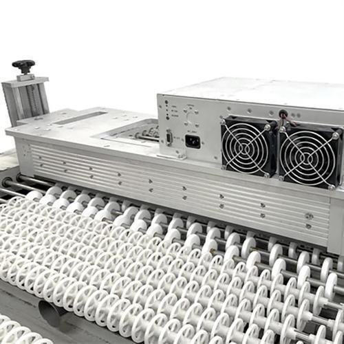
- Dielectric Barrier Discharge (DBD) Plasma Electrodes
- Design With High Plasma Density.
- Direct Plasma Design with Single Electrode. (Air-Cooling)
- Using Ar for Reaction Gas. Electrode width can be designed based on customers' requirements.
- Electrodes can be expanded with higher treatment speed.
- Gap between Electrode and Substrate is about 1 ~ 4 mm.
- Can be Sheet by Sheet or Reel-to-Reel treatment.
- Can be standalone machine or module intregrated with in-line mechanism.
- Single Side Treatment. Reaction Gases: Ar (Low Gas Rate Needed). Gap Between Electrode and Substrate can enlarged to 4~5 mm. Plasma Effective Width: 100 mm ~ 1000 mm. (Can be larger based on customers' requirements). Treatment Speed: 0.5 ~ 5 m / min in general (Can be changed based on customers' requirements). Suitable for various materials with sheet or film forms. High Plasma Treatment Stability and Uniformity.
- Surface Cleaning and Surface Modifications for PCB Panels before Gold Plating, Copper Plating or Shipping.
- Suitable for Surface Cleaning/Modification For Bare Glass or ITO Glass.
- Suitable for LCD/Sensor Cleaning For Touch Panel Applications. Suitable For Panel Cleaning (Replacing UV Ozone Cleaner To Save Costs) in Color Filter Applications. (Bare Glass/ITO Glass Cleaning, Before BM, Before R, G, B Photoresist Processes). Electronic and Non-electronics Devices Plasma Treatment With Metal or Non-Metal Materials. (e.g. PI, PET, PE, Plastic).
- Film Growth Applications.